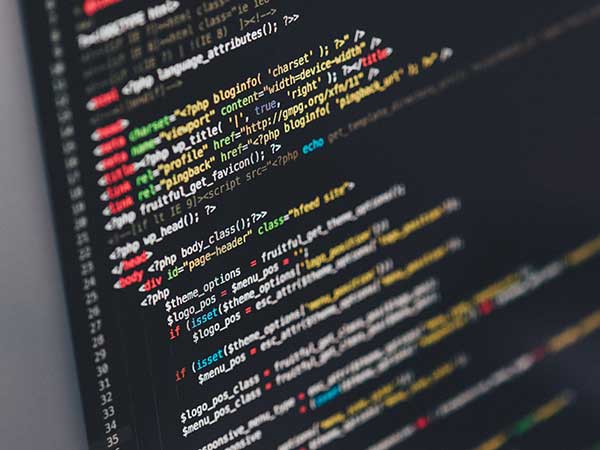
Recent IoT electrical trends in 2021 will prove that the digital market for interrelated smart devices is hiking rapidly, and the PCB designers will have to rethink their strategies to fulfill these needs for a new era. Making or building this new facility needs synthesizing and modifying the certain best methods starting from the basics of a high-speed outlook, PDN built-up, strong and bold flex to flex outlook, and mechanical start.
Getting an idea on this, how can the PCB building designers easily develop a dual IoT outlook and cope up with the needs in the market trends? Here are some of the wide changes we see in the PCB outlook for certain IoT based appliances. We hope that the PCB designers who are newly starting to step into the extensive world of IoT appliances can easily grab hold of the opportunities to excel in the field and innovate their thinking skills.
Digital Market Needs and Factors
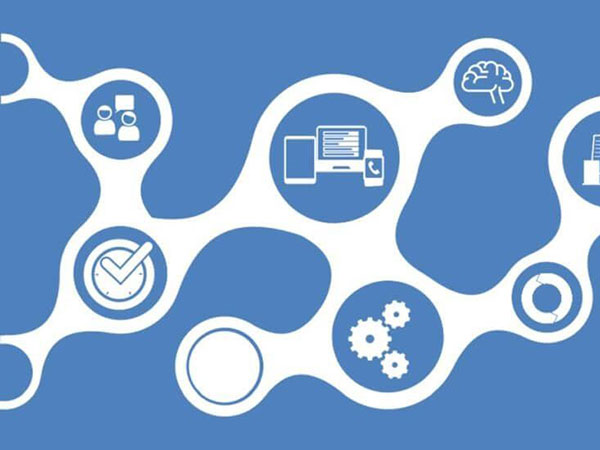
The IoT digital market changes put forth several remarkable issues on the PCB designers. Systematic and operational devices need smaller, enhanced, more effective product designs suitable to the modern advancements in the recent IoT technology. From the perspective of features, the newly made IoT devices will come with functionality that has not been seen in the earlier facilities. These are inclusive of the features regarding wireless communications, voice, image identification, enhanced video plus audio facilities, and urgent needs for coping up with a chain of regulated sensors and the touch of HMI tools.
Moreover, the IoT devices can be considered some real chip imbibed systems with a wide range of functions. Thus the PCB designers will be required to enhance or facilitate much more about the need for certain software to bring these devices into a working condition. The PCB designers would be purely given instructions on familiarizing themselves with as many coding languages as possible, starting from the ground level idea about C/C++ to advanced knowledge on Python and other networking frameworks.
To start up the operations and functions needed in so many newly formed IoT devices, we should take care of four crucial designing changes moving deeper into the mainstream:
- Extensive use of the HDI outlooks
- Extensive use of the bold flex as well as flex ideas
- Addition of several wireless abilities to communicate
- Additive production at a larger scale
- Productivity analysis for the better manufacturing process
Practices of designing concerning HDI
Needs for several smaller appliances and more operation oriented devices need the greater application of the HDI designing modules. The HDI boards are located with just as many issues for the building executives as they do for the designers’ sector, and we will begin to observe a higher use of the HDI approval to balance the small sizes of the board. The enhancement of newly made and interconnected chains will be supported by adding several manufacturing services for the PCBs with specific reference to the IoT applications.
As part of the HDI designing and routing channel, we will begin to notice even larger counts in the layer, with small traces of the networking signal situated in the PCBs’ interior parts that have already been packed. This will help free up several valuable areas on the surface layers to grant some higher elements. In addition to these new interrelated chains, this also needs certain unique additive structures for the advanced equipment to ensure it remains low. The power is low, and the elements can easily communicate in the concerned board without any ambiguity.
Bold and Strong PCB Outlook
The extensive use of fully transparent and bold circuits grants a newly made board to precisely conform to its allotted materials. It enhances some elements to move along with their boundaries as per the requirement. This explains the urge to build groups for collaboration with a more effective path during the designing phase. The hardware and electronics engineers can no further seek to confine themselves and work on other parts of some newly made devices. They will forcibly have to join together in a box of a single framework chain of electrical and mechanical outlook factors to develop higher and advanced IoT products.
Advanced Wireless Opportunities
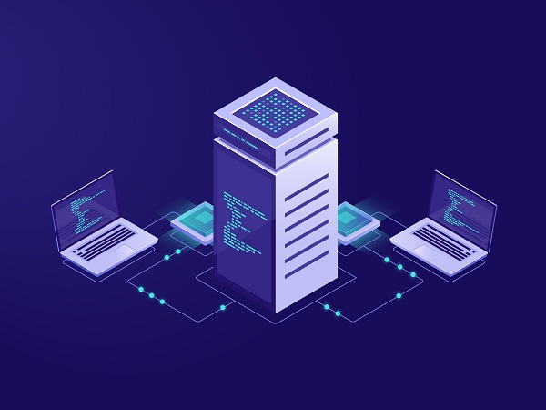
Let’s turn the clock back to smartphones, for the time being. One should understand that modern phones already reach each other via cellular data, WiFi option, Bluetooth facility, and in some cases, the NFC option. Certain devices for several applications, especially at the end user level, will require to be compatible with the feature of 5G as various cellular frameworks build up. Some of the enhancement boards are pre-equipped with the compatibility with cellular protections, granting the designers to develop the chip imbibed services connected to a normal cellular data network. Several applications, such as the surrounding or technical handling, will most likely be inclusive of other wireless facilities protocols.
The Update to the Production of Additive Features
The capability to print certain 3D designs is considered functional electronic devices and are already on their way to revolutionize the rapid advancement in prototyping, enact various visual customization, and provide a helping hand to shorten the development cycle chains. As more elements, as well as services, come in the online firm in the near schedule, we can easily expect to observe a higher shift to the use of various additive production at a greater scale, including for the PCBs, electronic-based devices, and even the devices which utilize the semiconducting facility.
The world is nowadays getting more advanced every day. More and more appliances are coming, including a range of sensors, communication abilities, and network framework options. Even an older man can easily take control of his listening aids from his fingertips. The hardware designing executives will have to rethink the electrical plus mechanical factors of their new interface simultaneously. This is to be done so that just attaching a capacitor at a location or setting an extra chip at the place will not be hectic anymore.